| GMEK's Technology |
|---|
 |
| Patented |
 |
| Under R&D |
 |
| Custom Tailored |
 |
| Bookcase |
G.MEK Patented Technologies
Pt Thin Film Technology
(1) Control of Crystallographic Orientation of Pt Thin Films
Pt thin film has generally a strong (111) crystallographic orientation of its grains because the surface energy of (111) crystallographic plane of a FCC (Face Centered Cubic) unit cell of Pt film is the lowest among major crystallographic planes such as (100), (220) and (111). Therefore, during sputtering, the deposited Pt film grows on the substrate wherein (111) crystallographic planes of Pt grains are laid to be parallel to the substrate surface. In order to deposit Pt film with the other crystallographic orientation, for example, (200)-oriented grains except (111) grains, the substrate of (100) MgO single crystal must be used because lattice constant of (100) plane of a Pt unit cell is very similar to that of (100) plane of a MgO unit cell so that the Pt film to grow preferably in (200) orientation by virtue of good lattice matching between them. Similarly, highly (100)-oriented MgO film as a buffer layer on Si substrate allows Pt film to preferably grow in (200) orientation. However, the conventional technique using a single crystal or a buffer layer as a substrate to control the preferred orientation of Pt film has a disadvantage of making the process expensively and inconveniently.
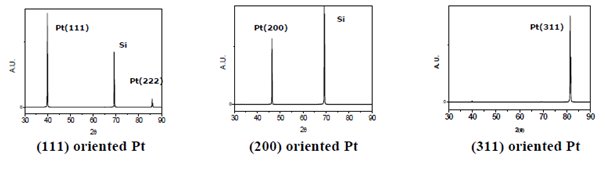
GMEK has a novel technique to control the crystallographic orientation of Pt film in (111), (200), (220), and (311)-direction as the film deposited on various kinds of substrates including oxidized Si wafer by reactive sputtering.
(2) Control of Microstructure of Pt Thin Films
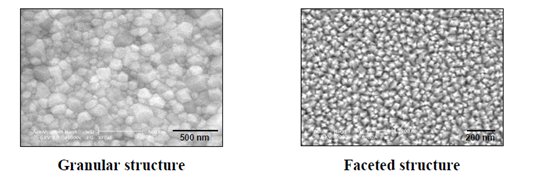
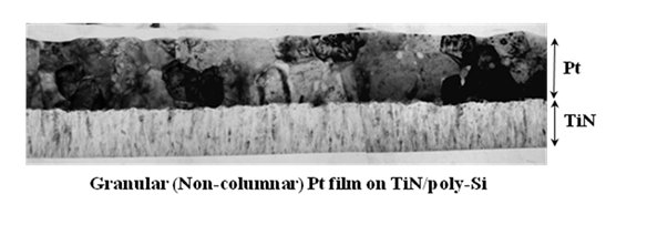
It is very important to control the microstructure of Pt film because the microstructures of thin films, in general, strongly affect the device performance. GMEK has a unique technique of changing the microstructure of Pt films widely from granular structure to faceted structure via columnar structure. Hence, we can provide Pt films responding to various customer needs.
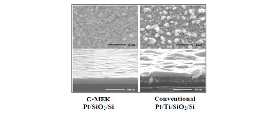
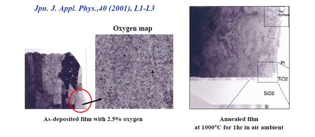
(3) High Thermal Stability of Pt Thin Film
Pt thin film has widely been used as an electrode for various kinds of devices including high dielectric capacitors and piezoelectric sensors. To obtain excellent physical and electrical properties, the devices need annealing treatment during fabrication in oxygen ambient at high temperature of 650℃ and above. Unfortunately, during the annealing process, degradation of device properties occasionally occurs due mainly to peel off of Pt film from substrate or interdiffusion between constituent elements of the film and the substrate. The thin film technique of GMEK experienced in semiconductor industry over 15 years can provide our customers with thermally stable Pt thin films on oxidized Si wafers such as Pt/Ti/SiO2/Si and Pt/TiO2/SiO2/Si.
(4) Giant Grain (GG) Growth Technology
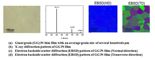
We can change the average grain size of Pt film from sub-micron to a few tens of microns. In addition, in case of utilizing our intellectual propriety technique named as giant grain (GG) growth technique, extraordinary giant grains with average grain size of a few hundreds to a few thousands of microns can be formed. The crystallographic orientation of GG Pt film can also be controlled in the direction of either (111) or (200) or (220). It is expected that the GG Pt film can induce epitaxial growth of a functional film when it is used as a bottom electrode. The GG Pt film can also be exploited in various kinds of device application such as Pt RTD sensor, IR sensor, and MEMS device.
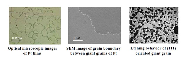
The GG growth of Pt film was accomplished by post annealing treatment at a temperature of 1000℃ in air ambient after depositing Pt film by reactive sputtering using a mixed gas of Ar + O2.
The figures shown below describe the results of (a) optical microscophic observation, (b) X-ray diffraction (XRD) anlaysis, (c) Electron Backscatterd Diffraction (EBSD) analysis in normal direction, and (d) Electron Backscatterd Diffraction (EBSD) analysis in transverse direction, respectively. As can be seen, it is clearly shown that the GG Pt film was composed of exaggerated grains with (111) crystallographic orientation.
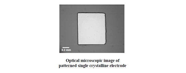
The figure shown below exhibits an optical micrograph of patterned Pt electrode composed of single crystal-like single grain, which was prepared by our GG Pt technology. It is presumable that a functional film is able to grow epitaxially on patterned GG Pt electrode.
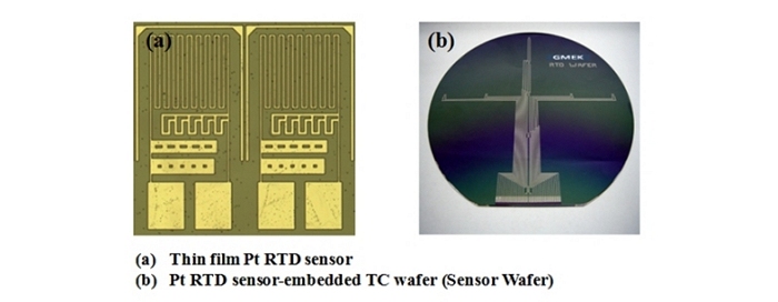
GMEK has recently developed the prototype of thin film-type Pt RTD sensor and Pt RTD sensor-integrated TC wafer by exploiting our intellectual propriety of GG Pt technology and continue to conduct research for commercialization in near future.