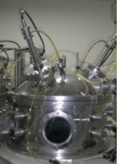
We have a wide experience and a deep knowledge in thin film technology, especially sputtering process, of semiconductor business over 15 years.
We can deliver a variety of sputter-deposited thin films on substrates with various type and size to customers as follows.
 Menu of Sputtering Foundry Service
| Menu | Materials | Film Thickness | Substrate |
|---|---|---|---|
| Common Metals | Cu, Ti, Cr, Ni, Al, Si, Ru, Ta, W, Mo |
Typical thickness : < 1 um (The film thickness over 1 um is also possible according to film materials. Hence, please, ask us before request.) |
Type: - Si wafers - Single crystals - Glasses - Ceramics - Metal plates - Plastics, etc. Size: - (max) dia: 8 inches (200 mm) - A piece of substrate also possible |
| Noble Metals | Au, Ag, Pt, Pd | ||
| Nitrides | TiN, TaN | ||
| Oxides | SiO2, TiO2, Ta2O5, RuO2, NiO | ||
| Other Materials | NiCr, Ta-SiO2 |
- The foundry service fee per substrate will be changed depending mainly on sputter target materials, film thickness, substrate type and size, and order quantity.
- Please, send e-mail or post a question in Q&A bulletin board or call us if you have a question on our sputtering foundry service.
| Type | Crystallographic Orientation of Pt | Thickness (nm) | Si Wafer (Substrate) | |||
| SiO2 | Glue layer | Pt | ||||
| 1 | Pt/SiO2/Si | (111) | 300 | none | 150 | P-type (100) |
| 2 | (200) | 300 | none | 150 | ||
| 3 | Pt/Ti/SiO2/Si | (111) | 300 | 10 | 150 | |
| 4 | Pt/TiO2/SiO2/Si | (111) | 300 | 20 | 150 | |
| 5 | (200) | 300 | 20 | 150 | ||
- Thickness of each layer can be changed upon request.
- Pt films on the other substrates are also available.
| Type | Thickness (nm) | Substrate | Application | ||
| Au | Glue | ||||
| 1 | Au/Cr | 43 | 5 | Most types of substrates are available. | MEMS devices, Piezo devices |
| 150 | 10 | ||||
| 2 | Au/NiCr/Ti | 200 | 500/400 | ||
- Thickness of each layer can be changed upon request.
| Type | Thickness (nm) | Substrate | Application | ||
| Cu | Glue | ||||
| 1 | Cu/Ti | 500 | 200 | Most types of substrates are available. | MEMS devices, Seed Cu layer |
| 2 | 300 | 100 | |||
- Thickness of each layer can be changed upon request.


 Specification of Standard Pt wafers
 Specification of Au films
 Specification of Cu films